The indispensable requirements for the components of today’s millimeter-wave communication facilities (including satellite communication) are their small weight, small size, low cost, and high reliability. The first two requirements are very easy to meet if microstrip lines are used as waveguide systems. However, these lines cannot compete with hollow metal waveguides in the transmission of power signals. This poses the problem of the development of a manufacturing technology that would provide a reasonable degree of integration of simple elements into multifunctional units and devices. Such a technology must have a low cost and a short production time, give products with identical electrodynamic characteristics, and be implementable by means of standard equipment.
The microwave component manufacturing technology developed at the Institute of Technical Mechanics of the National Academy of Sciences of Ukraine and the National Space Agency of Ukraine meets these requirements. This technology is based on multilayer electroforming whose distinctive features are electroforming assembly and a special electrodeposition regime. The former makes possible near-monolithic microwave multifunctional modules, while the latter provides the fine-grain structure, plasticity, and strength of the deposited metal.
An important constituent of the successful implementation of this technology is complex yet sectional reusable matrices, which made possible quasi-monolithic multifunctional devices without butt joints. We have experience in the use of this technology in the manufacturing of generator modules, decouplers, horn antennas, and monolithic multifunctional devices based thereon.
Owing to multilayer electroforming, a finished product possesses a sufficient mechanical strength while its mass and size are a fraction of those of its all-metal counterpart.
This wasteless waveguide-integration technology may be an alternative to traditional ones. In addition to a considerable reduction in mass and size (the waveguide wall thickness is 200 to 300 μm, as distinct from several millimeters in traditional devices), this technology offers a far lower adjustment cost because it provides not only high manufacturing accuracy but also repeatable geometrical and electrical characteristics of millimeter-wave units.
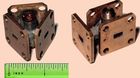
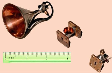
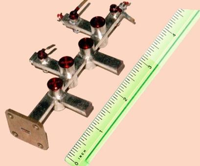
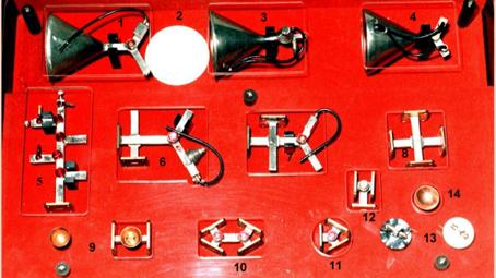
The efficiency of this technology in the manufacturing of highly engineered functional units of a transmit/receive system has been demonstrated by the example of three-port circulators (Fig. 1), a transmitting module with a small-size electrically controlled generator (Fig. 2), a millimeter-wave generator with a two-stage power amplifier (Fig. 3), and a set of components and units for communication systems (Fig. 4).